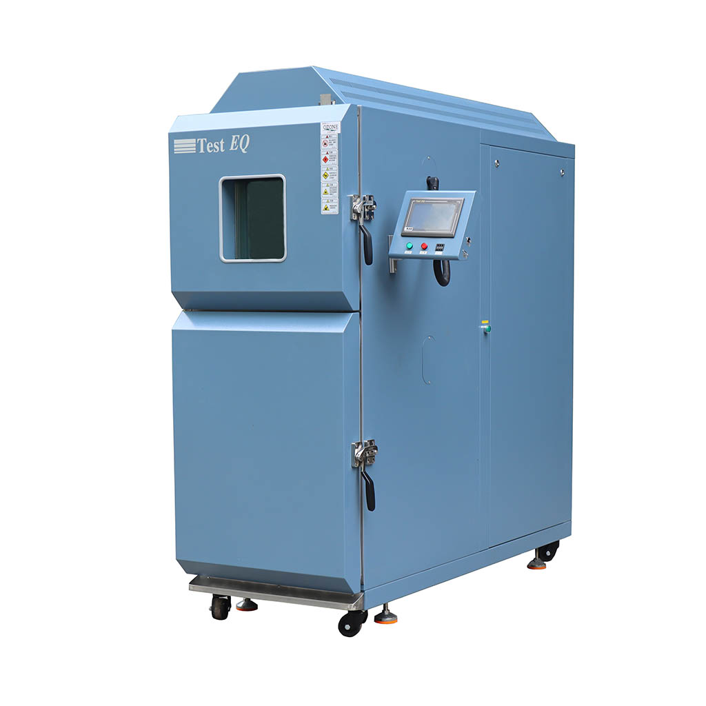
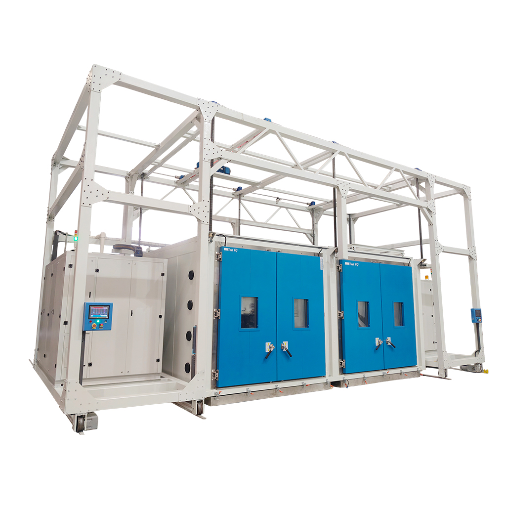
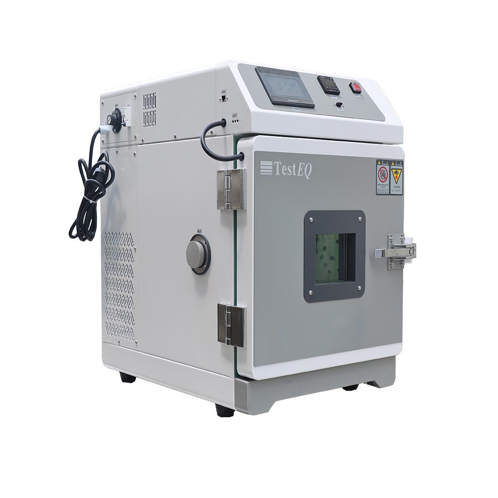
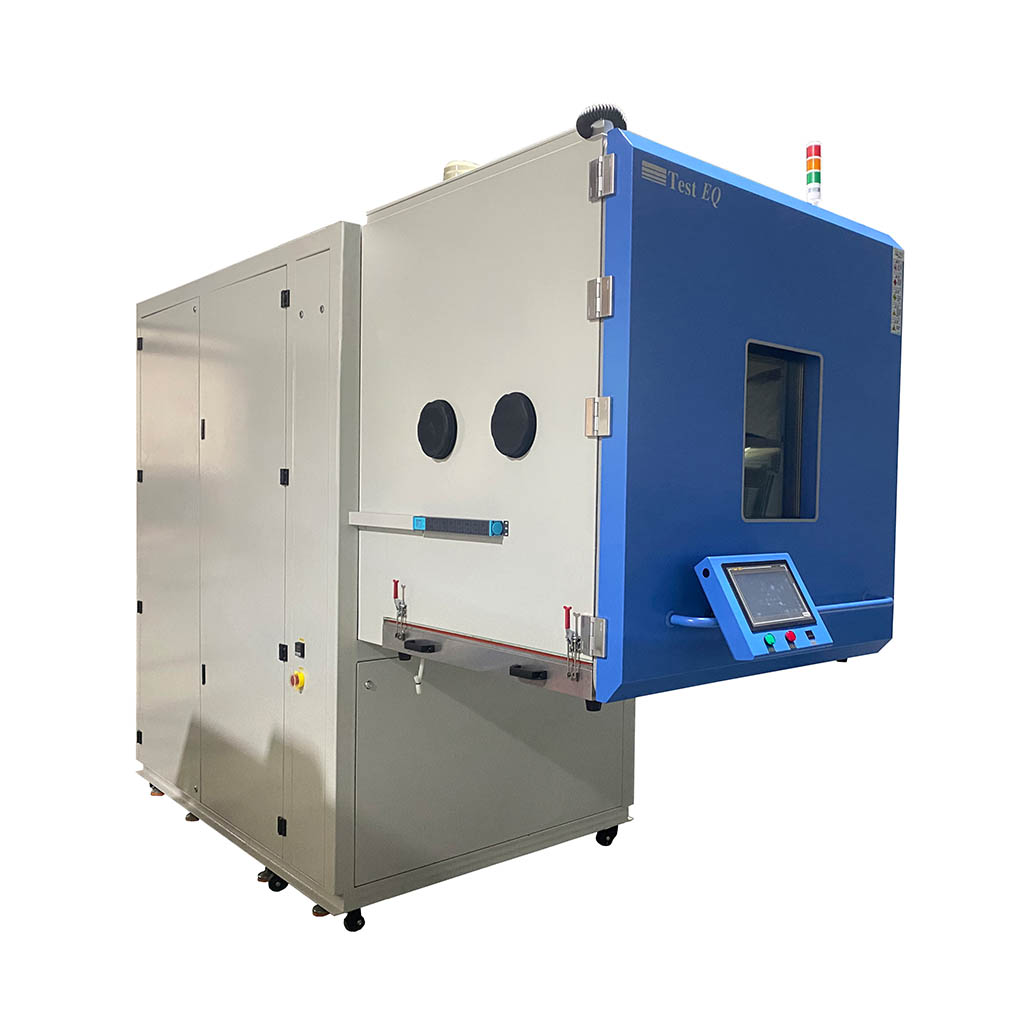
Overview:
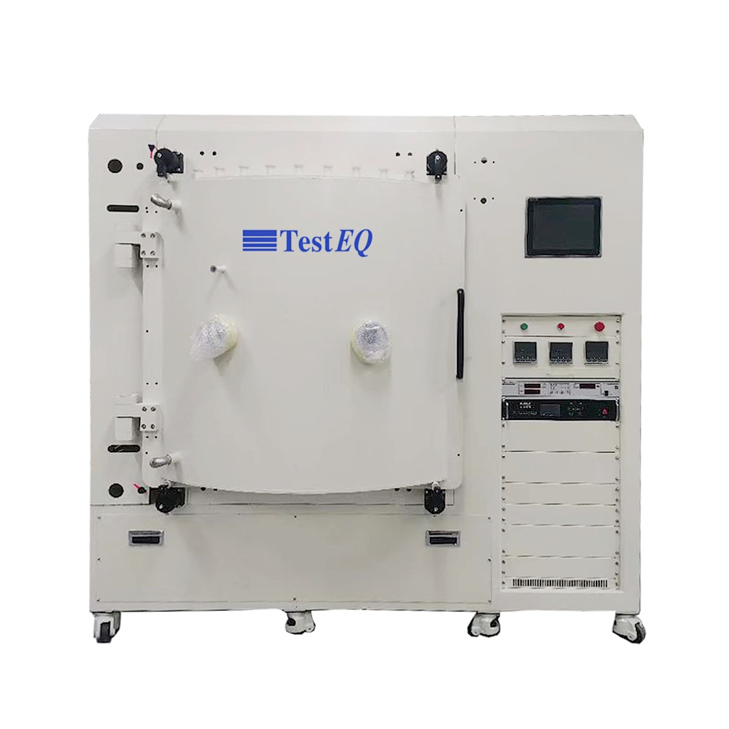
The Thermal Vacuum Cleaning System is an advanced industrial cleaning solution designed for precision degreasing, contamination removal, and high-purity surface treatment under controlled thermal and vacuum conditions.
By integrating controlled heating, vacuum extraction, and optional inert gas purging, the system removes oils, organic residues, moisture, and outgassing contaminants from complex components while minimizing surface damage and secondary contamination risks.
This technology is widely applied in aerospace, semiconductor manufacturing, precision optics, vacuum equipment, and other industries requiring strict cleanliness control.
What is a Thermal Vacuum Cleaning System?
A Thermal Vacuum Cleaning System is a dry precision cleaning technology that uses elevated temperature and reduced-pressure environments to remove molecular-level contaminants from high-value components.
Unlike conventional wet cleaning or solvent-based processes, thermal vacuum cleaning does not rely on chemical agents or physical contact. Instead, contaminants are thermally activated, evaporated, and extracted through a controlled vacuum process.
The system is commonly used for:
- Semiconductor manufacturing components
- Aerospace precision parts
- Optical assemblies
- Vacuum chamber components
- High-reliability electronic assemblies
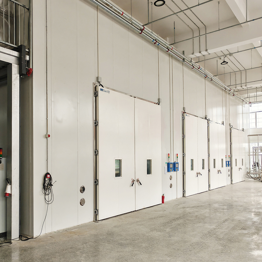
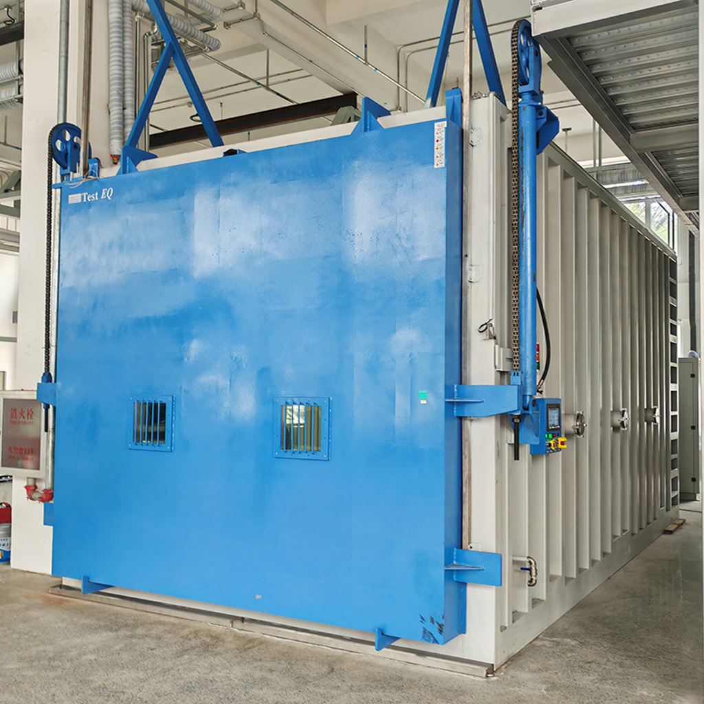
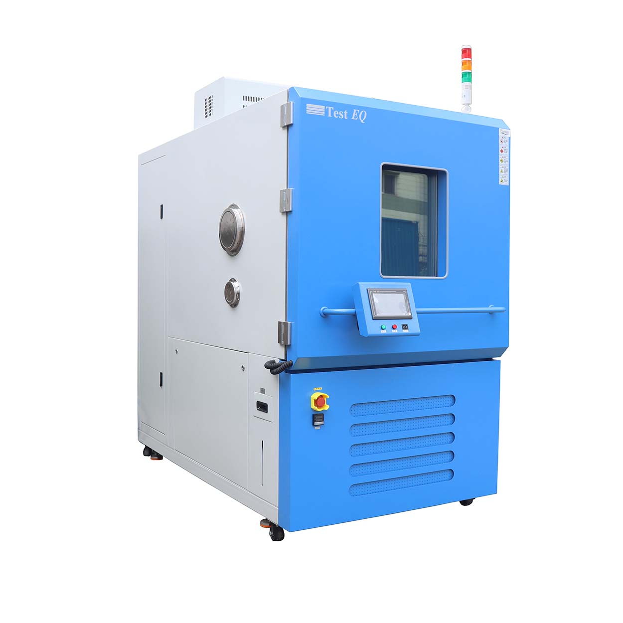
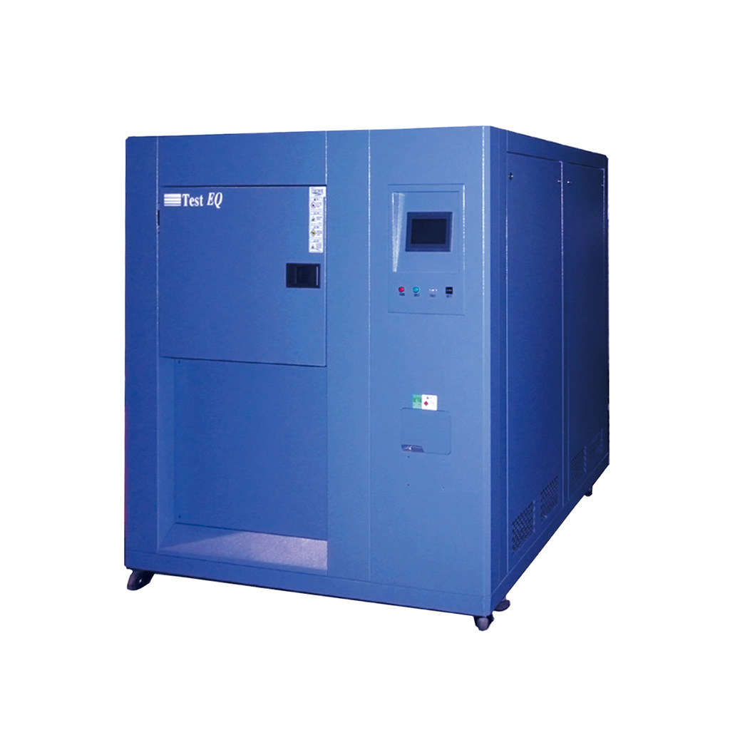
For applications requiring ultra-clean surfaces and contamination control, TestEQ provides customized thermal vacuum cleaning systems with configurable chamber size, temperature control, vacuum level, and automation options.
Working Principle:
The system operates under a combined process of:
Under high vacuum (typically 10⁻² to 10⁻⁵ mbar), the boiling point and adsorption energy of contaminants are significantly reduced.
Controlled heating (typically 80°C to 450°C depending on material) increases molecular mobility and breaks weak surface bonds.
Contaminants transition into gas phase and are continuously removed via vacuum pumping systems.
Under low-pressure conditions, contaminants are more easily separated from surfaces, while thermal energy accelerates the cleaning efficiency without damaging the substrate.
This process is widely used in outgassing reduction and ultra-clean surface preparation in aerospace and semiconductor industries.
How Does Thermal Vacuum Cleaning Work?
A Thermal Vacuum Cleaning System removes contaminants through a controlled combination of heating, vacuum extraction, and purification processes. The main working steps include:
1. Loading and Vacuum Chamber Sealing
Components are placed inside the cleaning chamber, and the chamber is sealed to create a controlled vacuum environment. This prevents external contamination and ensures stable cleaning conditions.
2. Vacuum Pressure Reduction
The system reduces internal pressure to accelerate the evaporation and release of volatile contaminants, including moisture, oils, and organic residues.
3. Controlled Thermal Activation
Precise heating increases the molecular activity of contaminants, helping release trapped substances from complex surfaces, gaps, and internal structures without damaging sensitive components.
4. Contaminant Evaporation and Extraction
Released contaminants are converted into volatile compounds and removed through the vacuum pumping system, achieving efficient dry cleaning without chemical solvents.
5. Purification and Gas Purging
Optional inert gas purging can be applied to remove remaining particles and improve surface cleanliness, reducing the risk of secondary contamination.
6. Cooling and Clean Component Removal
After completing the cleaning cycle, the system performs controlled cooling before the components are removed, ensuring stable temperature conditions and high-purity surface treatment.
Thermal Vacuum Cleaning vs Traditional Cleaning Methods
| Method | Limitation | Thermal Vacuum Advantage |
|---|
| Solvent Cleaning | Chemical residue risk | Dry process, no contamination |
| Ultrasonic Cleaning | Micro-damage risk | Non-contact process |
| Plasma Cleaning | Surface etching | No surface modification |
| Thermal Vacuum Cleaning | Higher cost | Ultra-clean, no residue, deep desorption |
Thermal vacuum cleaning is the only method combining thermal activation + vacuum desorption physics.
Why Thermal Vacuum Cleaning is Superior
Compared with traditional cleaning methods:
No chemical solvent residue
Lower environmental impact
Higher cleaning precision
Suitable for micro-structures
Safer for sensitive components
This makes it ideal for next-generation precision manufacturing
Industry Benefits
Improves product reliability
Reduces contamination-related failure rates
Enhances semiconductor yield rate
Extends lifespan of precision components
Supports clean manufacturing compliance
Industry Standards Compliance
This system is designed in accordance with:
ASTM E595 – Total Mass Loss (TML) and Collected Volatile Condensable Material (CVCM)
SEMI Standards – Semiconductor contamination control guidelines
ISO 14644 – Cleanroom and contamination classification
MIL-STD-810 – Environmental engineering test procedures
Compliance ensures compatibility with aerospace and semiconductor qualification processes.
Why TestEQ Thermal Vacuum Cleaning System
TestEQ designs thermal vacuum cleaning systems for high-precision industrial environments requiring strict contamination control.
Engineering Advantages:
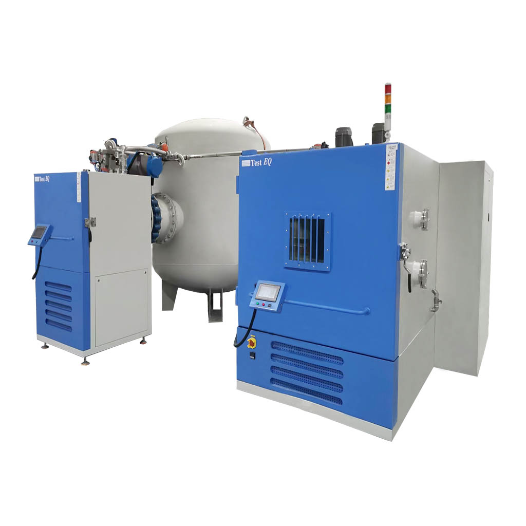
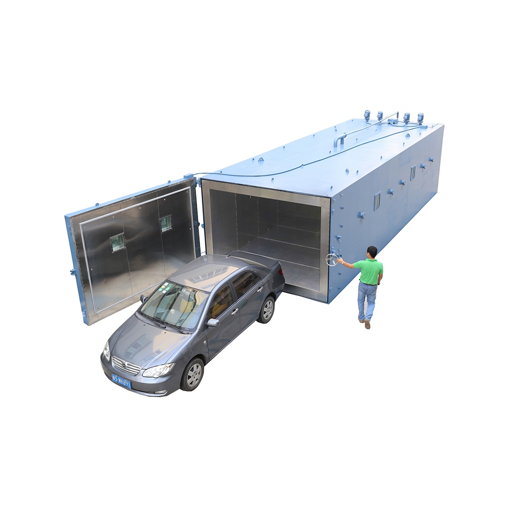
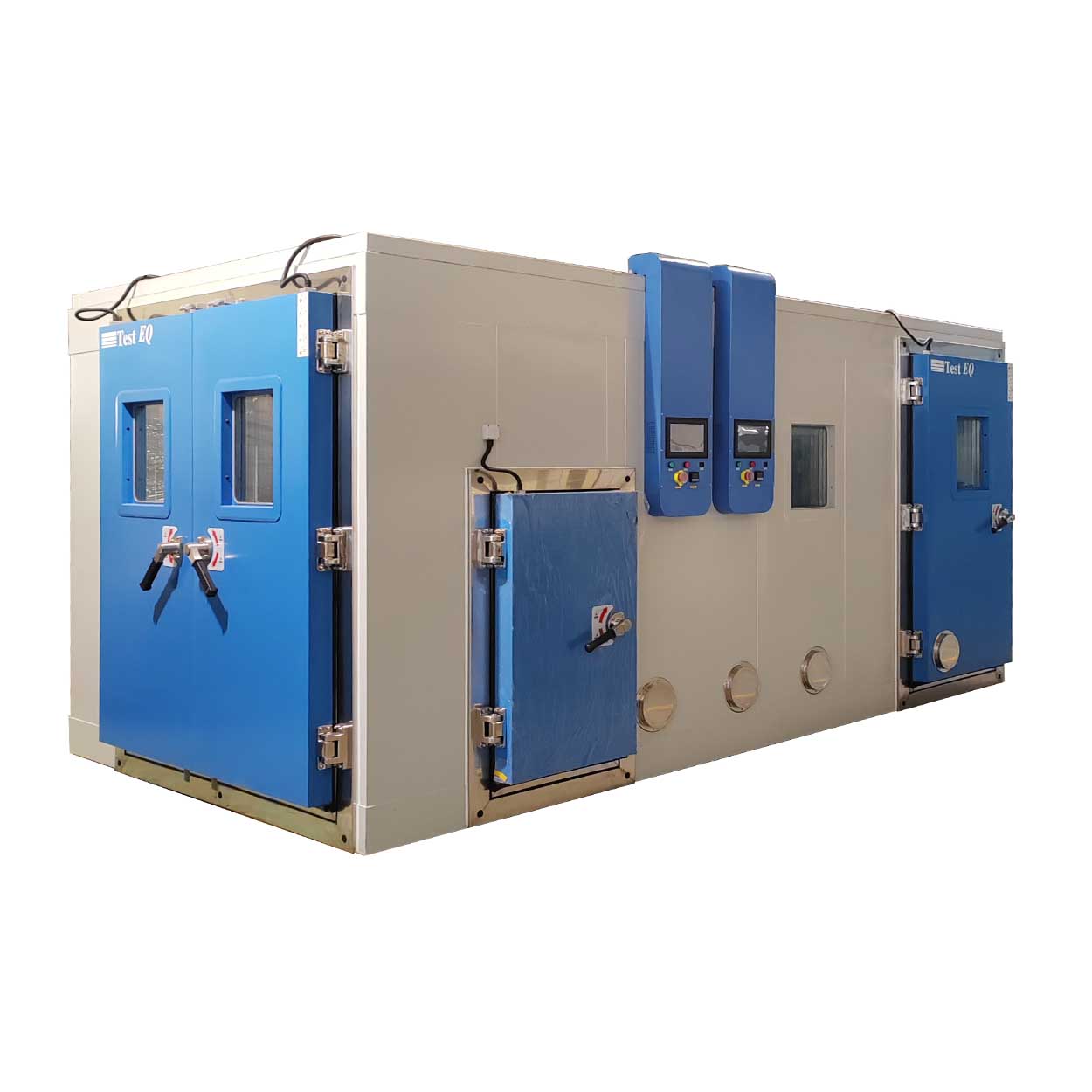
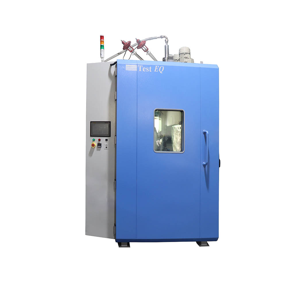
Custom vacuum chamber design (non-standard sizes supported)
Optimized thermal uniformity control system
Low outgassing structural engineering
Integration with thermal vacuum test systems (TVAC compatibility)
Application Experience:
Aerospace qualification testing systems
Semiconductor reliability chambers
Precision laboratory vacuum systems
Optional Configurations
FAQ:
1.What is a thermal vacuum cleaning system?
It is an industrial system that uses vacuum pressure and thermal energy to remove contaminants from precision components.
2.What is vacuum degreasing?
Vacuum degreasing is a process that removes oil, grease, and residues under low-pressure conditions without chemical solvents.
3.Which industries use thermal vacuum cleaning systems?
It is widely used in aerospace, semiconductor, optical manufacturing, automotive, and medical industries.
4.What are the advantages over chemical cleaning?
It eliminates chemical waste, improves precision, and reduces contamination risk.
5.Can it be customized?
Yes, systems can be customized for chamber size, vacuum level, and temperature range.
6.Is thermal vacuum cleaning better than ultrasonic cleaning?
Yes, because it is a dry, non-contact process that avoids mechanical vibration and chemical residues.
7. What contaminants can a thermal vacuum cleaning system remove?
A thermal vacuum cleaning system can remove various volatile and organic contaminants, including oils, hydrocarbons, moisture, grease residues, and outgassing substances from precision components. The cleaning capability depends on the material properties, contamination type, temperature profile, and vacuum conditions.
8. How does a thermal vacuum cleaning system ensure cleaning consistency?
A thermal vacuum cleaning system ensures repeatable cleaning results through precise control of temperature, vacuum pressure, heating rate, and process parameters. Automated monitoring and recipe-based operation allow manufacturers to maintain stable cleaning performance for high-volume production and critical components.
Internal Linking Module
Recommended Equipment
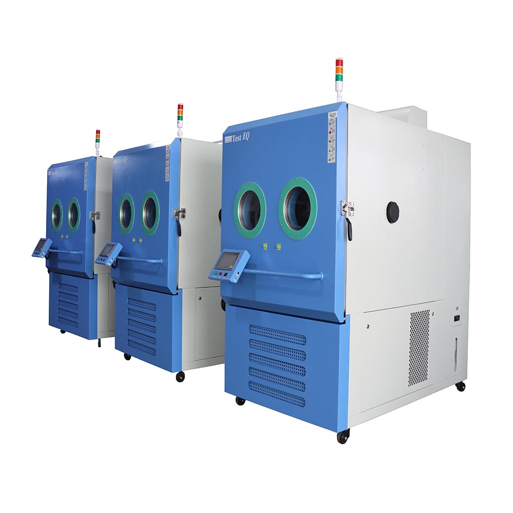
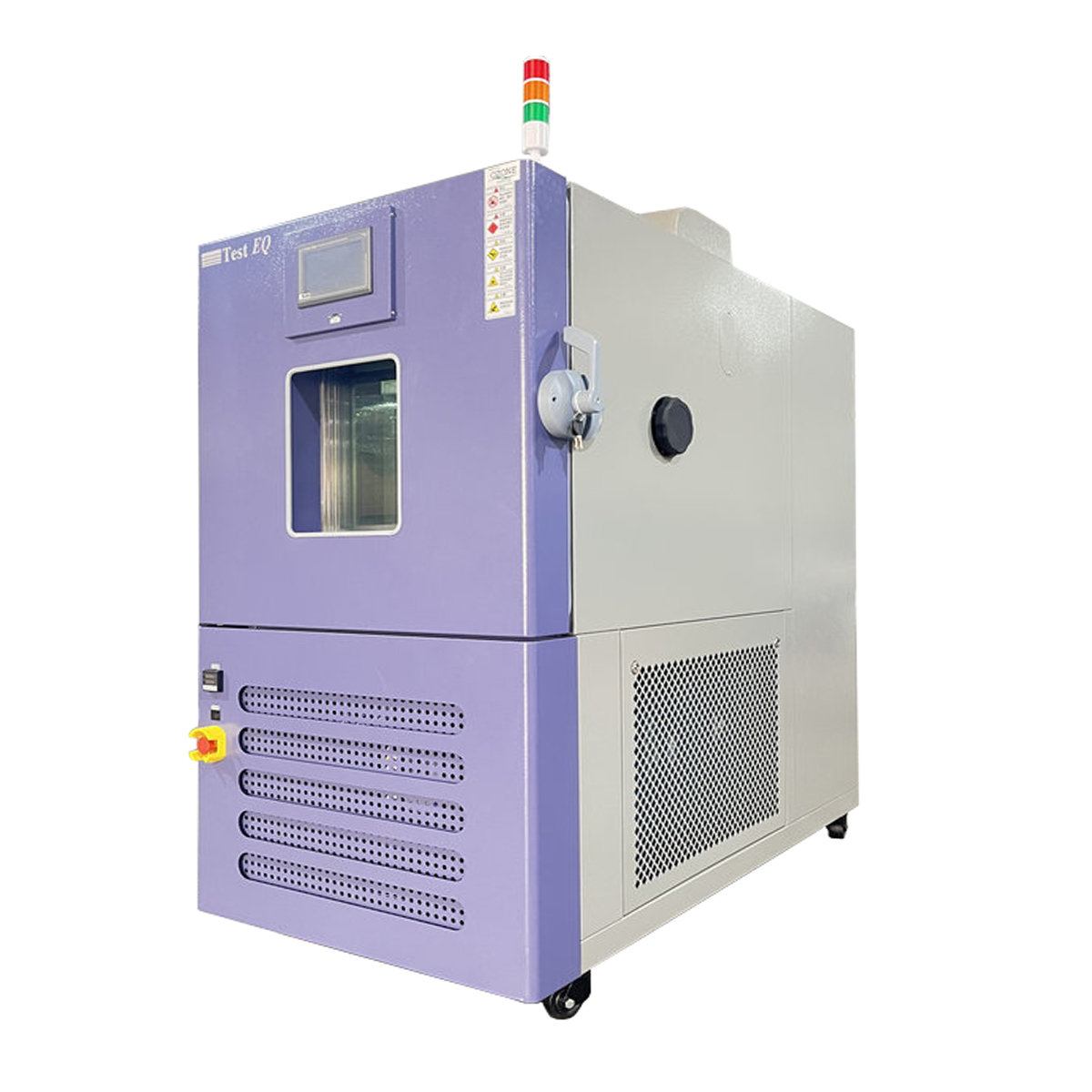
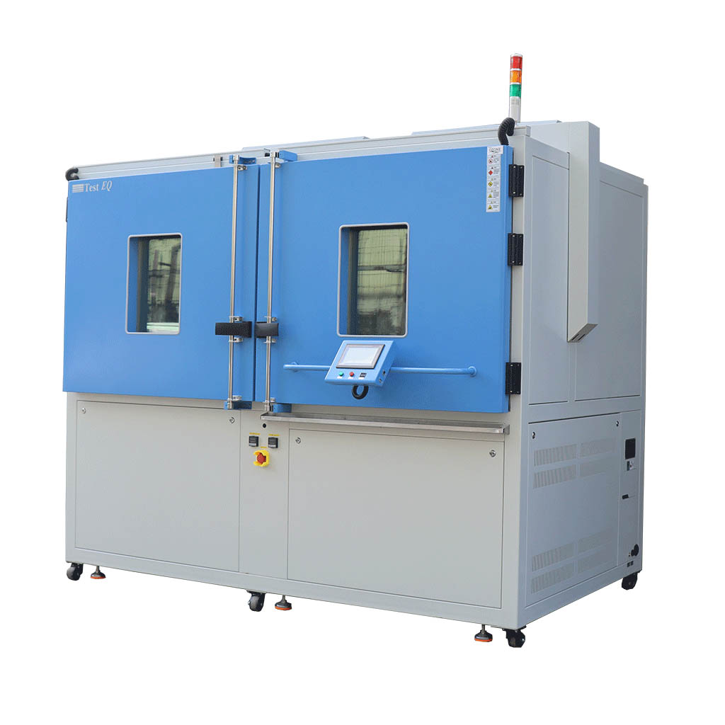
Advanced thermal vacuum systems used to simulate outer space conditions including high vacuum, extreme temperature variation, and radiation-like thermal stress. Essential for satellite components, spacecraft subsystems, and aerospace material validation.
Environmental test system used to simulate repeated temperature transitions between extreme high and low conditions. Widely applied in electronics, automotive components, and semiconductor reliability testing to identify fatigue and failure mechanisms.
Related Standards
Military standard defining environmental engineering and testing procedures including thermal, vibration, shock, humidity, and vacuum conditions. Commonly used for defense, aerospace, and ruggedized electronics qualification.
International standard specifying environmental testing procedures for electronic and electrotechnical products, including temperature cycling, humidity exposure, and mechanical stress tests.
Semiconductor industry reliability standards used to evaluate electronic component durability under thermal cycling, humidity stress, and accelerated life testing conditions.
Related Resources
This article explains how temperature and low-pressure (altitude) environments are simulated in reliability testing systems. It provides insight into how aerospace, semiconductor, and electronics industries validate product performance under extreme combined thermal and vacuum conditions.