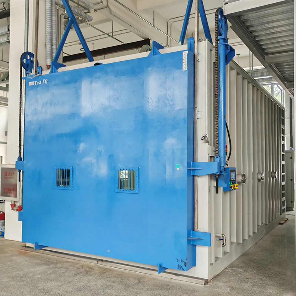
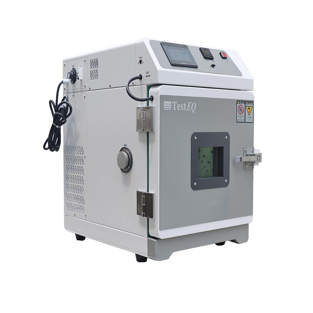
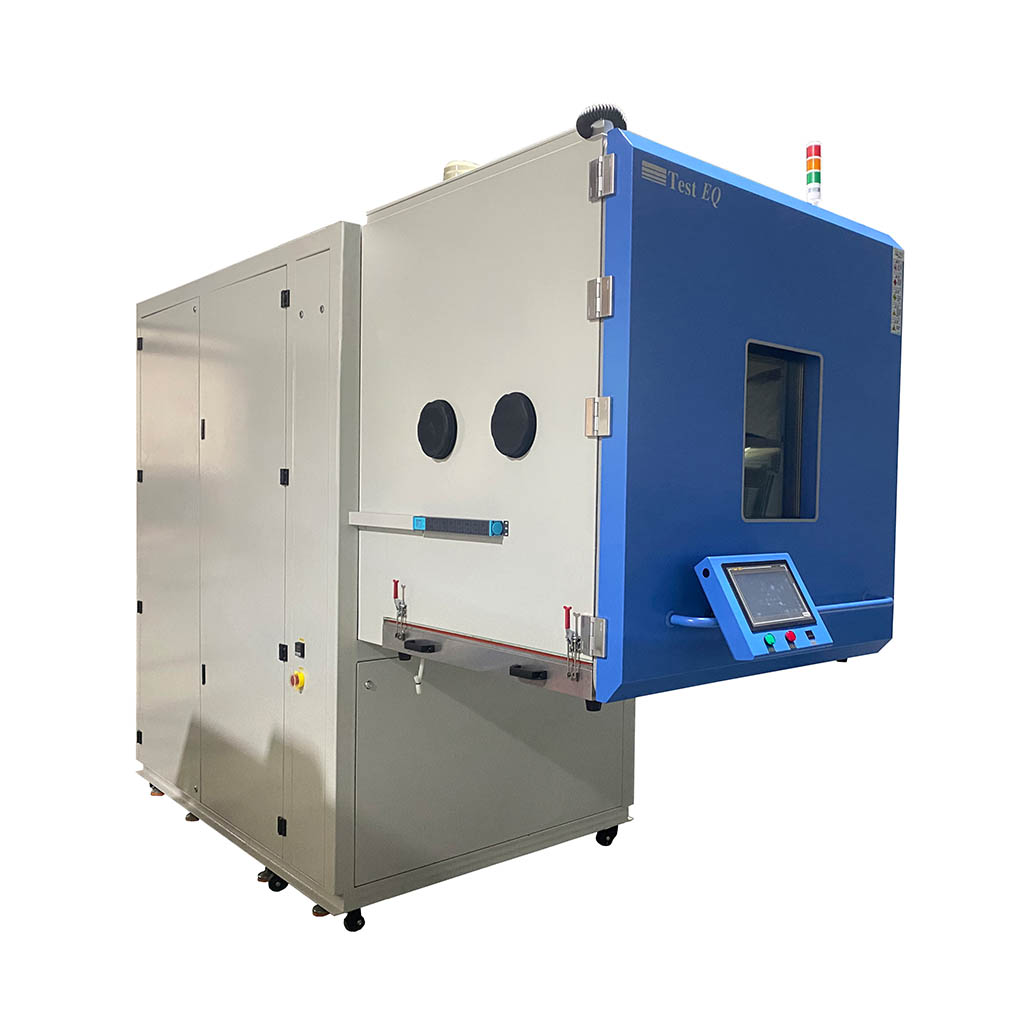
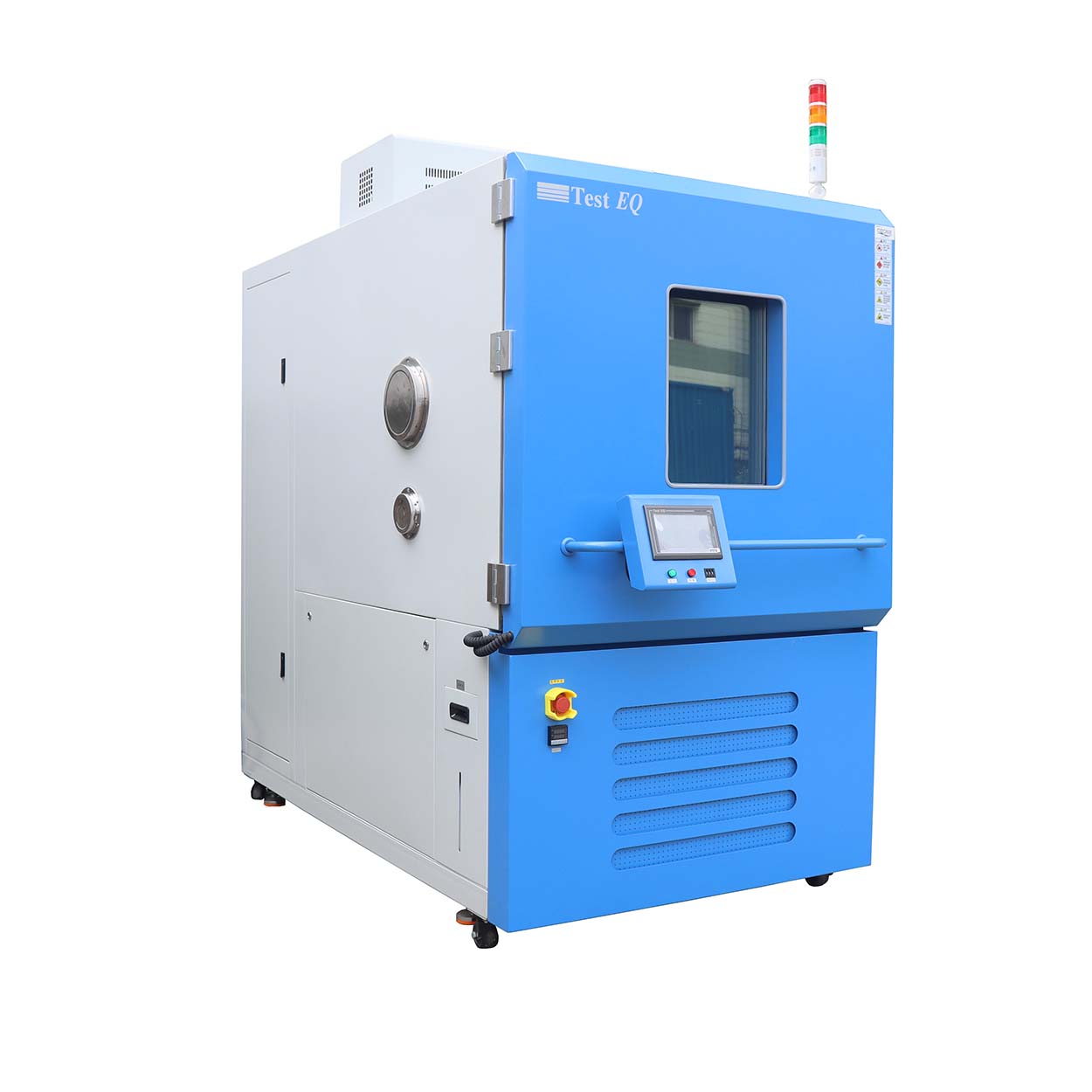
Semiconductor Oven for Wafer & Semiconductor Equipment Thermal Processing
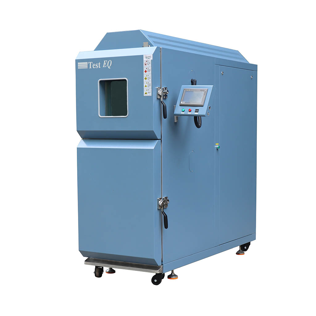
TestEQ Semiconductor Ovens are engineered thermal processing systems for semiconductor manufacturing, wafer processing, semiconductor packaging, and advanced electronics production.
The systems provide controlled heating, drying, baking, curing, and thermal stabilization for semiconductor materials and components where temperature uniformity, process repeatability, contamination control, and equipment integration are important.
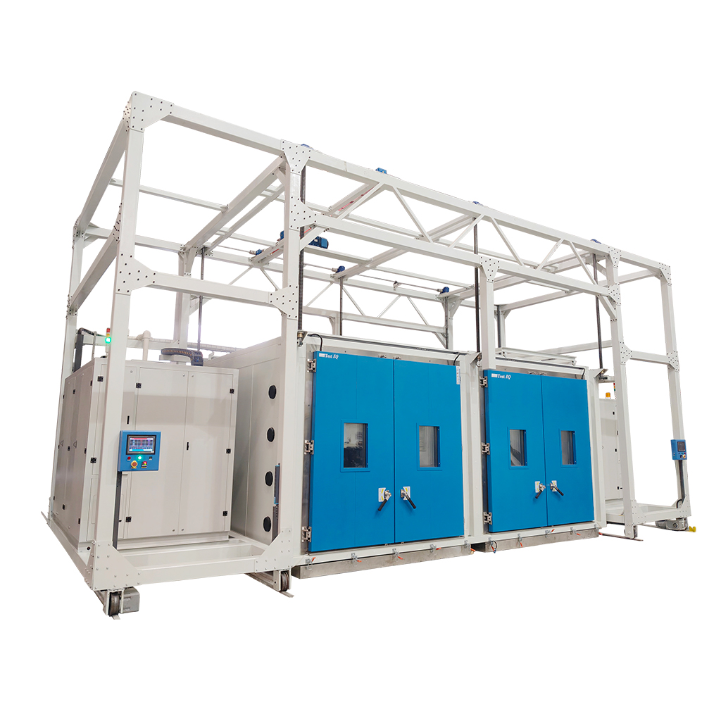
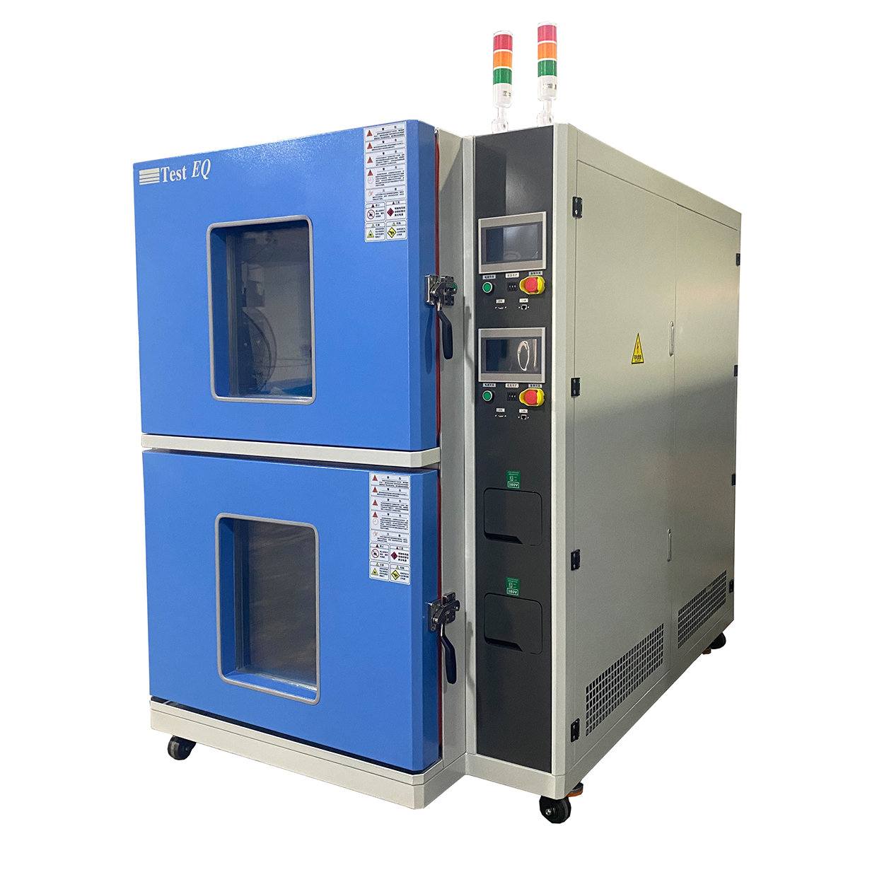
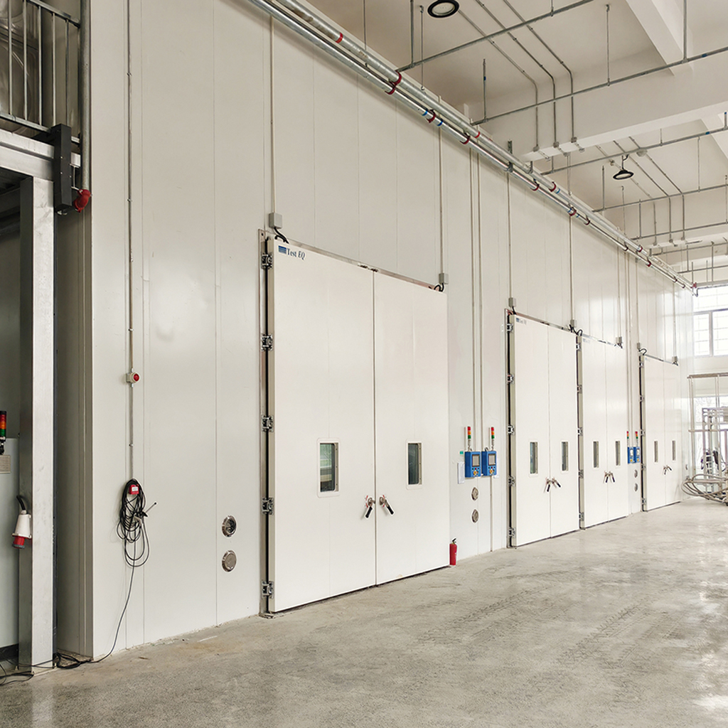
Available configurations include cleanroom-compatible ovens, nitrogen-purge ovens, high-temperature ovens, vacuum-assisted configurations, multi-zone systems, and customized thermal processing equipment for semiconductor equipment manufacturers.
Semiconductor Oven for Semiconductor Equipment Applications
A semiconductor oven is a precision thermal processing system used as part of semiconductor manufacturing and packaging processes.
Unlike a conventional industrial oven, a semiconductor equipment oven must be designed around the thermal requirements of the process, the material being processed, the required cleanliness level, airflow distribution, loading method, and production interface.
Typical requirements include:
• Stable and repeatable temperature control
• High temperature uniformity
• Controlled airflow circulation
• Low particle generation
• Cleanroom-compatible construction
• Nitrogen purge capability
• Programmable thermal recipes
• Data logging and process monitoring
• Automatic loading and unloading options
• MES or factory automation integration
• Custom chamber dimensions and fixtures
TestEQ works with semiconductor manufacturers, packaging companies, laboratories, and semiconductor equipment integrators to develop thermal processing systems according to specific process and production requirements.
Typical Semiconductor Thermal Processing Applications
Wafer Baking and Dehydration
Controlled heating can be used for wafer dehydration and thermal baking processes where stable temperature conditions are required.
The oven can be configured for different wafer sizes, carrier systems, shelf arrangements, airflow requirements, and production volumes.
Photoresist and Polymer Thermal Processing
Semiconductor manufacturing processes may require controlled thermal treatment of photoresist, polymers, and related materials.
The oven can be configured for programmable temperature profiles and controlled airflow to improve process repeatability.
Semiconductor Packaging
Thermal processing is widely used in semiconductor packaging operations, including:
• Die attach curing
• Epoxy curing
• Underfill curing
• Package baking
• Polymer curing
• Post-molding thermal treatment
• Wire-bonding process preparation
For packaging applications, the chamber can be designed around product loading, fixture configuration, thermal mass, temperature uniformity, and cycle requirements.
Semiconductor Component Drying
Semiconductor components and materials may require controlled drying or moisture removal before subsequent manufacturing or reliability processes.
TestEQ ovens can be configured for controlled heating and optional nitrogen purge according to the material and process requirements.
Clean Thermal Processing
For semiconductor manufacturing environments, contamination control can be as important as temperature performance.
TestEQ can configure semiconductor ovens with suitable internal materials, airflow paths, sealing, filtration, and low-particle design according to the required clean manufacturing environment.
Semiconductor Oven for Semiconductor Equipment Integration
For semiconductor equipment manufacturers, the oven can be developed as an integrated thermal processing module rather than a standalone laboratory oven.
Possible integration options include:
• Automatic wafer loading
• Automatic product transfer
• Conveyor or carrier integration
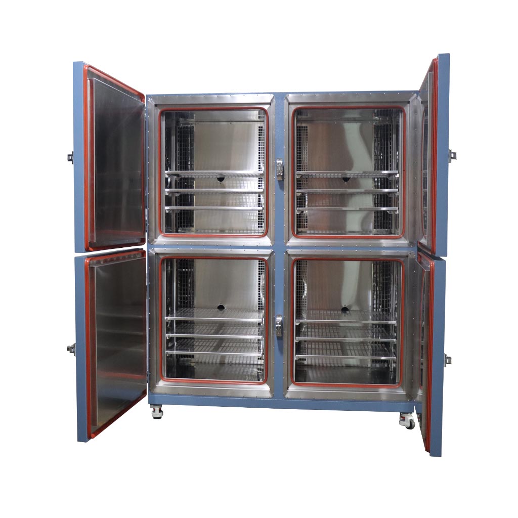
• Multi-chamber configurations
• Recipe management
• PLC control
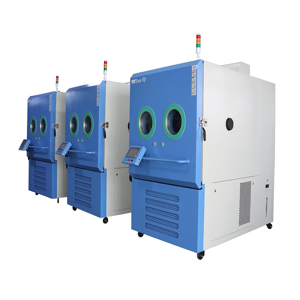
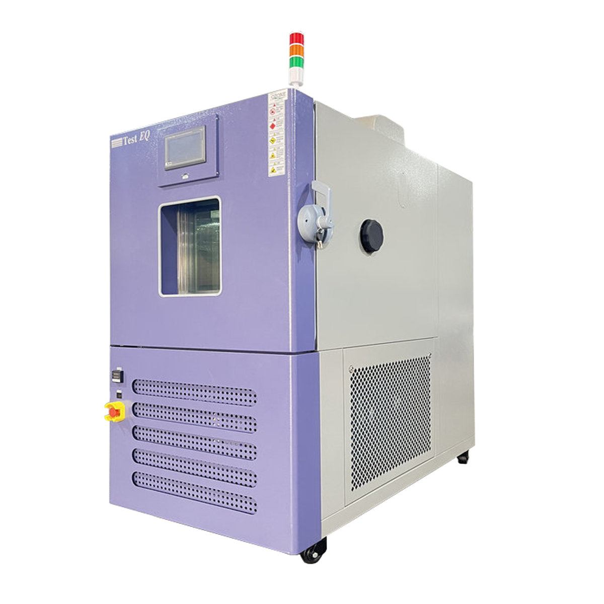
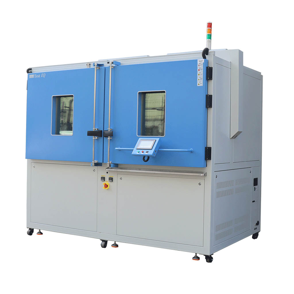
• Touchscreen HMI
• Data logging
• Remote monitoring
• MES communication
• Factory automation interfaces
• Customized fixtures and shelves
The equipment architecture can be adapted to the customer's process flow, available installation space, throughput requirements, and automation strategy
Nitrogen Purge Semiconductor Oven
Nitrogen purge is available for processes where controlled atmospheric conditions are required.
An N₂ purge system can be used to reduce exposure to ambient air during thermal processing and help control oxidation or moisture-related process conditions.
The nitrogen system can be customized according to:
• Nitrogen flow requirement
• Chamber volume
• Purge sequence
• Oxygen monitoring
• Process temperature
• Product loading method
• Automatic control requirements
For semiconductor applications, the N₂ system can also be integrated with the oven controller and production automation system.
Temperature Performance
TestEQ semiconductor ovens are available in different temperature configurations according to the thermal process.
Typical configurations include:
• RT to 200°C standard configuration
• Up to 300°C customized configuration
• Higher-temperature configurations available for specific applications
| Parameter | Typical Configuration |
|---|
| Temperature Range | RT to 200°C |
| Higher Temperature | Up to 300°C; customized options available |
| Temperature Fluctuation | ≤ ±0.5°C |
| Temperature Deviation | ≤ ±2.0°C |
| Heating Method | Electric heating with SSR control |
| Temperature Sensor | K-type thermocouple |
| Controller | PLC / Touchscreen |
| Atmosphere | Air circulation or optional N₂ purge |
| Chamber Structure | Stainless steel |
| Shelves | Multi-layer, customized configuration |
| Automation | Optional |
| Data Logging | Optional |
| MES Integration | Optional |
Actual performance should be specified according to chamber size, load configuration, product thermal mass, process temperature, and customer acceptance criteria.
Semiconductor Oven Temperature Uniformity
Temperature uniformity is a critical parameter when selecting a semiconductor thermal processing system.
A suitable oven should maintain consistent thermal conditions across the effective working area rather than only achieving the set-point temperature at one measurement location.
TestEQ uses controlled airflow circulation, heating control, temperature monitoring, and chamber configuration to develop the required thermal distribution.
For a production project, the final temperature uniformity specification should be defined together with:
This approach allows the oven to be engineered around the actual process instead of relying only on an empty-chamber specification.
Cleanroom-Compatible Semiconductor Oven
Semiconductor production environments can require stricter control of particles, materials, airflow, and equipment interfaces than conventional industrial heating applications.
TestEQ can provide cleanroom-compatible configurations with:
• Stainless steel internal surfaces
• Low-particle design
• Controlled airflow
• Suitable sealing
• Cleanroom-compatible construction
• N₂ purge
• Customized loading interfaces
• Production automation integration
The required cleanliness classification and particle specification should be defined according to the customer's manufacturing process and facility requirements.
Semiconductor Oven vs Standard Industrial Oven
| Comparison Item | Semiconductor Oven | Standard Industrial Oven |
|---|
| Primary Purpose | Designed for semiconductor manufacturing processes, including wafer baking, drying, curing, and precision thermal processing | Mainly used for general industrial heating, drying, and curing applications |
| Main Applications | Semiconductor wafers, IC packaging, electronic components, photoresist curing, moisture removal, reliability preparation | Metal parts, coatings, plastics, general materials, industrial products |
| Temperature Control | High-precision temperature control with excellent stability and uniformity for sensitive semiconductor processes | Standard temperature control suitable for general industrial heating requirements |
| Temperature Uniformity | Optimized for strict thermal uniformity to reduce process variation and protect semiconductor materials | Usually designed for general heating consistency without semiconductor-level requirements |
| Contamination Control | Designed with low particle generation and clean processing requirements for semiconductor environments | Limited contamination control capability |
| Cleanroom Compatibility | Can be customized for cleanroom environments with suitable airflow design and materials | Usually not designed for cleanroom applications |
| Airflow Design | Optimized airflow circulation to achieve stable temperature distribution and protect wafer/component quality | Conventional airflow design focused mainly on heat transfer efficiency |
| Nitrogen Purge Capability | Supports optional nitrogen purge systems to reduce oxidation and protect moisture-sensitive semiconductor materials | Nitrogen protection is usually unavailable or not required |
| Process Repeatability | Provides high repeatability for semiconductor manufacturing and reliability testing processes | Suitable for less critical industrial heating processes |
| Control System | Often equipped with PLC control, touchscreen interface, data logging, and remote monitoring options | Usually uses basic temperature controllers |
| Particle Management | Focuses on minimizing particles and maintaining cleaner processing conditions | Particle control is generally not a primary design consideration |
| Product Requirements | Requires strict thermal performance, reliability, and process consistency | Focuses mainly on heating capacity and operational efficiency |
| Typical Industries | Semiconductor manufacturing, electronics, IC packaging, aerospace electronics, research laboratories | Automotive parts, metal processing, coating, general manufacturing |
| Investment Level | Higher investment due to precision control, clean design, and advanced monitoring requirements | Lower cost for standard heating applications |
Semiconductor Oven Selection Guide
When selecting a semiconductor oven, engineers and procurement teams should define the following parameters before requesting a quotation:
1. Product or Wafer Size
Specify wafer diameter, substrate dimensions, package dimensions, carrier size, or product fixture requirements.
2. Temperature Range
Define the minimum and maximum operating temperatures and the required temperature profile.
3. Temperature Uniformity
Specify the required uniformity across the effective working area under the actual product loading condition.
4. Atmosphere
Determine whether the process requires normal air circulation, nitrogen purge, controlled oxygen concentration, or another atmosphere.
5. Cleanliness
Define the required cleanroom environment, particle requirements, internal materials, and airflow configuration.
6. Loading Method
Specify manual loading, shelves, carriers, FOUP-related interfaces, automatic loading, or customized handling.
7. Throughput
Define the number of products or wafers per batch and the required cycle time.
8. Automation
For production equipment, determine whether PLC, MES, recipe management, data logging, remote monitoring, or factory automation interfaces are required.
9. Installation Requirements
Provide available footprint, power supply, exhaust requirements, nitrogen supply, facility interfaces, and cleanroom installation conditions.
Key Features of TestEQ Semiconductor Oven
Precision Temperature Control
Stable temperature control ensures consistent thermal processing and minimizes process variation during semiconductor manufacturing.
Cleanroom Compatible Design
The chamber structure supports semiconductor manufacturing environments where contamination control and low particle generation are critical.
Nitrogen Purge System
Optional nitrogen purge reduces oxidation risks and improves protection for moisture-sensitive semiconductor materials.
Low Particle Generation
Optimized airflow design helps maintain a cleaner processing environment for semiconductor applications.
Industrial Automation
PLC control, touchscreen operation and remote monitoring enable integration into modern smart manufacturing systems.
Why Choose TestEQ Semiconductor Oven
Unlike conventional industrial ovens, TestEQ Semiconductor Ovens are specifically designed for semiconductor production environments.
Benefits include:
• Excellent thermal uniformity
• Fast heating and recovery
• Reduced particle contamination
• Stable long-duration operation
• Energy-efficient airflow design
• Flexible chamber customization
• Support for clean manufacturing processes
• OEM solutions for semiconductor equipment manufacturers
Optional Configurations
• Nitrogen Inert Oven
• Vacuum Oven
• Class 100 Clean Oven
• High Temperature Oven
• Multi-Chamber Oven
• Automatic Loading System
• Data Logging System
• MES Communication Interface
Related Semiconductor Manufacturing & Reliability Standards
TestEQ Semiconductor Ovens can be configured to support thermal processing requirements associated with semiconductor manufacturing, packaging, and reliability qualification. Applicable standards depend on the specific process, product, and customer qualification requirements.
JEDEC JESD22 Reliability Standards — Common reliability test methods for semiconductor devices and packages.
JEDEC JESD22-A104 Temperature Cycling — Defines temperature cycling methods used for semiconductor reliability evaluation.
SEMI Standards — Relevant semiconductor manufacturing practices and equipment requirements, depending on the application.
The semiconductor oven should be specified according to the actual thermal process, temperature uniformity, atmosphere, cleanliness, loading method, and production requirements rather than a single standard alone.
Frequently Asked Questions
1.What is a semiconductor oven?
A semiconductor oven is a precision thermal processing system used for wafer baking, drying, curing, semiconductor packaging, and other controlled heating processes in semiconductor manufacturing.
2.What is a semiconductor oven used for?
Typical applications include wafer dehydration, wafer baking, photoresist or polymer thermal processing, semiconductor packaging, die attach curing, epoxy curing, underfill curing, and component drying.
3.Can a semiconductor oven be integrated into semiconductor equipment?
Yes. TestEQ can develop customized ovens with PLC control, automatic loading, product fixtures, data logging, MES communication, and other interfaces required for semiconductor equipment integration.
4.Can the oven use nitrogen?
Yes. An optional nitrogen purge system can be integrated according to the process requirements, including purge flow, sequence control, and monitoring.
5.Can the semiconductor oven be used in a cleanroom?
Yes. Cleanroom-compatible configurations can be developed with suitable internal materials, airflow design, sealing, and low-particle construction.
6.What temperature range is available?
The standard configuration supports approximately RT to 200°C. Configurations up to 300°C and other customized temperature ranges can be developed according to the application.
7.Can TestEQ customize the oven for wafers?
Yes. Chamber dimensions, wafer carriers, shelves, fixtures, airflow, nitrogen systems, loading methods, controls, and automation interfaces can be customized.
8.What information is required for a semiconductor oven quotation?
Procurement and engineering teams should provide the product or wafer size, temperature range, temperature uniformity, atmosphere requirements, cleanliness requirements, loading method, batch capacity, cycle time, available installation space, and automation requirements.
Internal Linking Module
Recommended Products
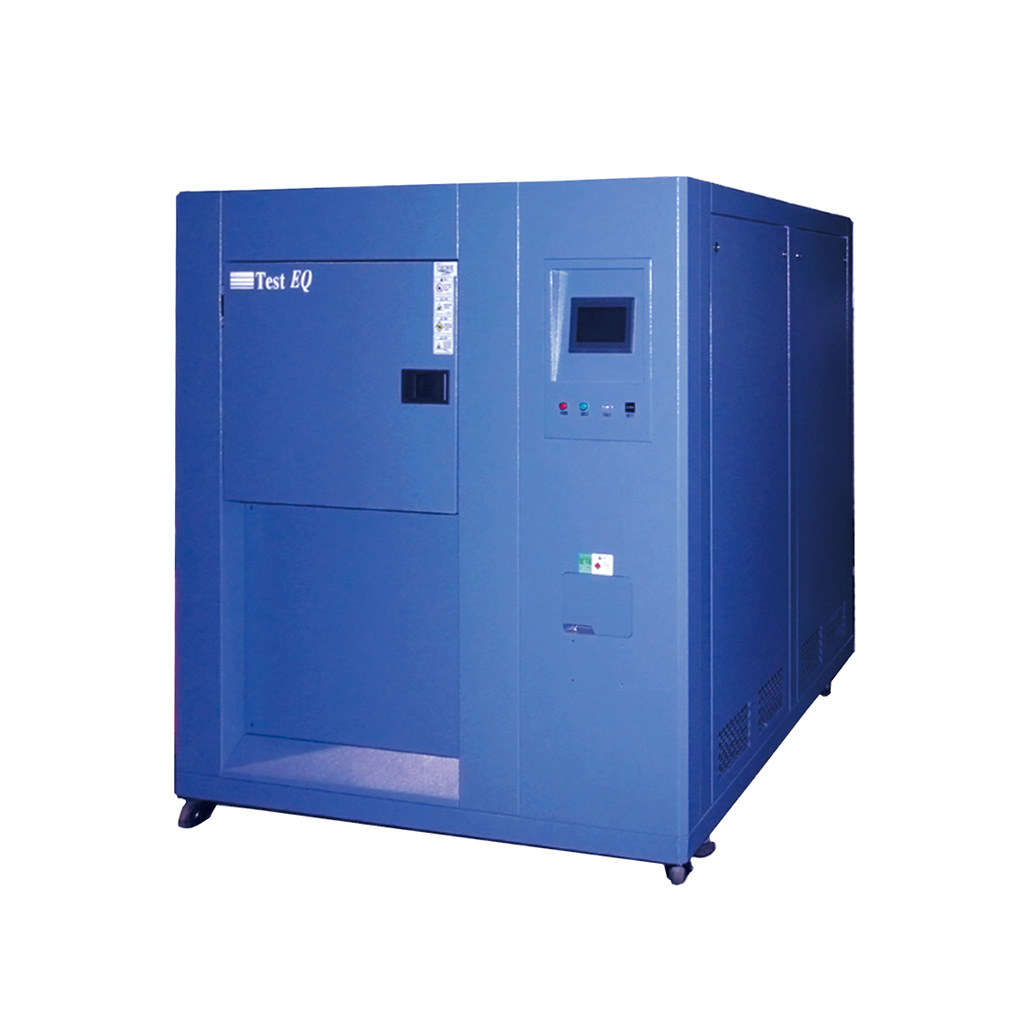
Designed to simulate repeated temperature changes for Environmental Stress Screening (ESS) and reliability validation. Suitable for semiconductor devices, PCB assemblies, automotive electronics, and aerospace components.
Perform rapid hot-to-cold temperature transition testing to evaluate thermal shock resistance, solder joint durability, and material reliability under extreme environmental conditions.
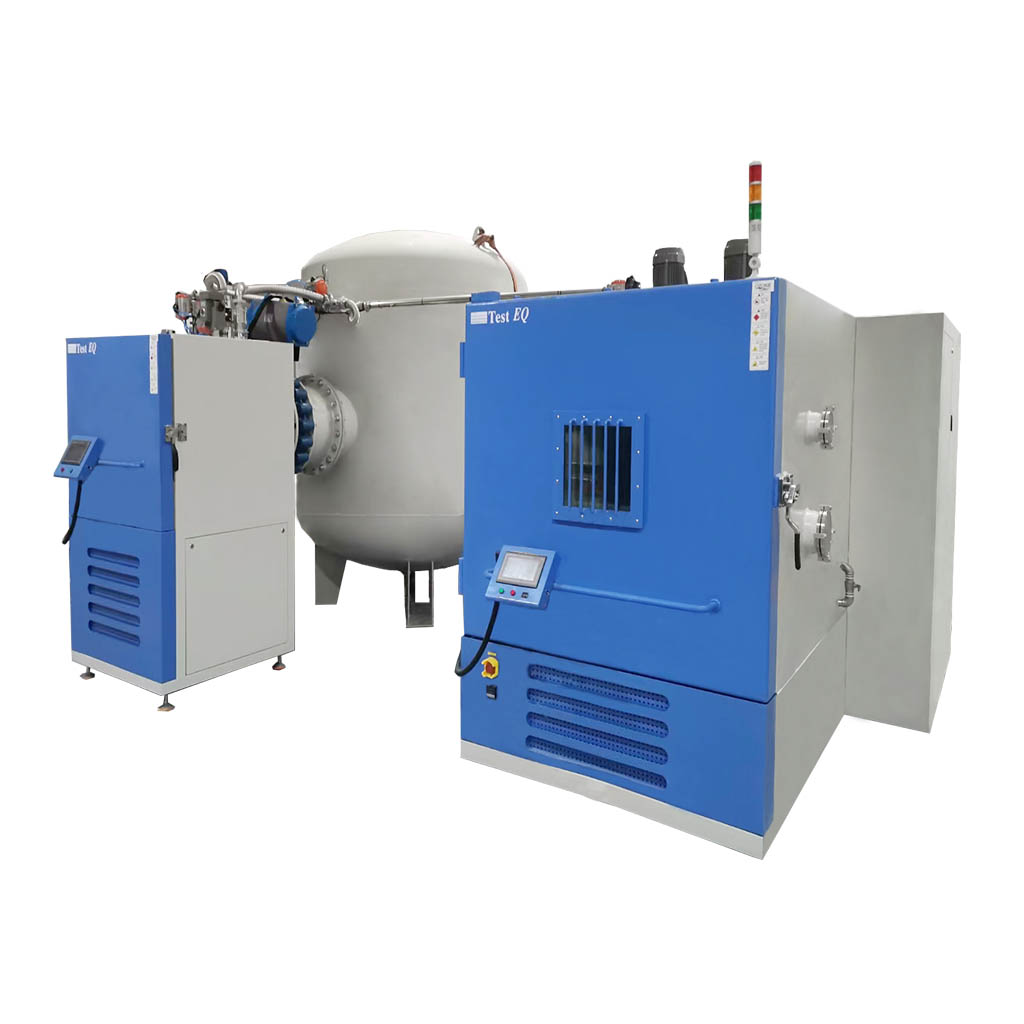
For accelerated temperature, humidity, and pressure stress testing of semiconductor packages.
Recommended Standards
Learn about the IEC 60068 series of environmental testing standards, including temperature, humidity, vibration, and thermal testing methods widely used for international product qualification.
Explore JEDEC JESD22 reliability test procedures for semiconductor devices, covering thermal cycling, thermal shock, moisture resistance, and accelerated life testing.
Temperature cycling methodology for semiconductor device reliability evaluation.
Related Resources
Discover common reliability tests used in semiconductor manufacturing, including temperature cycling, thermal shock, HAST, HTOL, and burn-in testing to improve product quality and long-term reliability.
Explains the difference between thermal cycling and thermal shock and when each test method is used.